Loading…
 ENDATA
>
ENDATA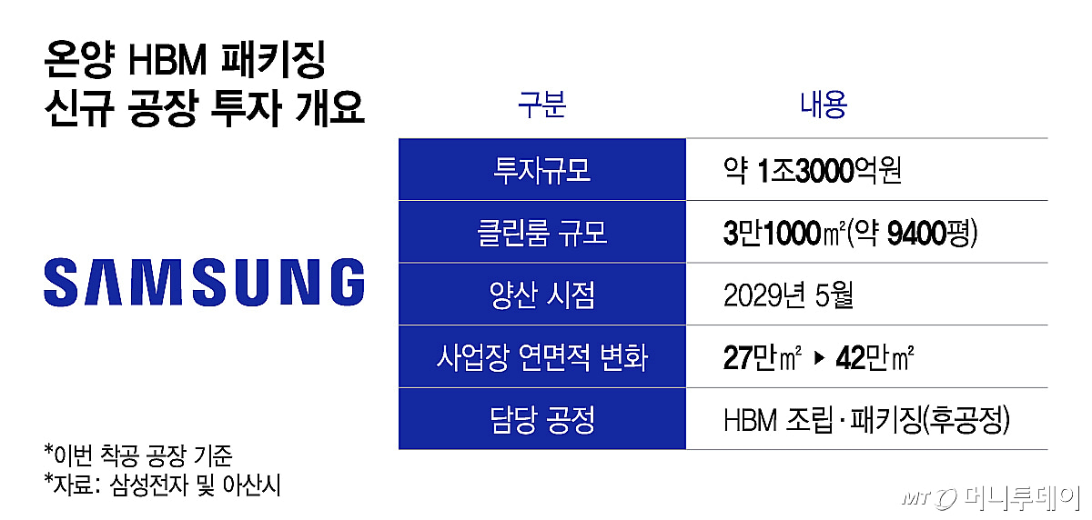
Samsung Electronics will hold a groundbreaking ceremony for a new HBM advanced packaging fab at its Onyang site in Asan, South Korea, investing approximately 1.3 trillion won. The facility will have a 31,000 sqm cleanroom and target mass production by May 2029.
“This marks a semiconductor speed-up campaign aimed at dispelling the AI bubble theory raised by some quarters.”mt.co.kr
Summarized from public sources; check the original articles before acting on it.